How to Read an Op Amp Datasheet
Abstract: This application note is a collection of operational amplifier (op amp) terms and their specifications. The article provides a handy reference guide for designers.
This glossary defines the operational amplifier (op amp) specifications that are commonly constitute in the Electric Characteristics Table of the typical op-amp data sail.
- Common-Way Input Resistance (RINCM)
For op amps operating in the linear region, this term defines the input common-mode voltage range divided by the change in input bias current across that range.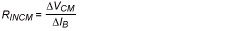
- DC Mutual-Mode Rejection (CMRDC)
This is a measure of the op amp'southward ability to refuse DC signals present in equal measure at both inputs. CMRDC can be calculated using the common-manner voltage range (CMVR) and the change in peak-to-peak input offset voltage beyond that range.
- AC Common-Style Rejection (CMRAir-conditioning)
CMRAir conditioning is a measure of the amplifier's ability to reject AC signals present in equal mensurate at both inputs. It is a function of differential open up-loop proceeds divided past common-mode open-loop gain. CMRAir-conditioning is usually specified at a given frequency and over a DC common-mode range.
- Proceeds-Bandwidth Product (GBW)
This is the constant product AOL * ƒ in the region of the -20dB/decade rolloff on the open-loop Gain vs. Frequency feature bend. - Input Bias Current (IB)
For op amps operating in the linear region, this term indicates the current that flows into the inputs, averaged. - Input Bias-Current Migrate (TCIB)
This is the modify in input bias electric current due to the change in temperature. TCIB is usually expressed in pA/°C. - Input Starting time Current (IOS)
This is the deviation betwixt the currents flowing into the two inputs. - Input Outset-Current Drift (TCIOS)
This is the modify in input offset current due to the change in temperature. TCIOS is usually expressed in pA/°C. - Differential-Mode Input Resistance (RIN)
This is the change in input offset voltage divided by the modify in input current. This change results from that changing voltage. For either input with the other input connected to a fixed common-mode voltage:
- Output Impedance (ZO)
For op amps operating in the linear region, this term indicates the small-scale-betoken internal impedance of the output final. - Output Voltage Swing (VO)
This term indicates the maximum peak-to-peak voltage swing that the output can attain without clipping the signal. 5O is ordinarily specified into a given load resistance and relative to the supply rails. - Ability Dissipation (Pd)
This is the quiescent power dissipated by the device under the given supply voltages. Pd is normally specified with no load attached to the output. - Power-Supply Rejection Ratio (PSRR)
This measures the ability of an amplifier to maintain its output voltage unchanged as the supply voltage varies. PSRR is ofttimes determined by measuring the change in input offset voltage every bit a result of the change in power-supply voltage.
- Slew Rate (SR)
This is the maximum large-point rate of modify of the output voltage divided by the amount of time that the change takes to occur. SR is usually expressed in V/µs, and sometimes listed separately for positive-moving and negative-moving signals. - Supply Current (ICC, IDD)
This indicates the quiescent current required by the device at the given supply voltage. These terms are usually specified with no load fastened to the output. - Unity Proceeds Bandwidth (BW)
This is the maximum frequency for which the open up-loop gain is greater than one. - Input Offset Voltage (VBone)
This indicates the voltage divergence that, when applied differentially to the inputs, causes the output to equal goose egg. - Input Offset-Voltage Migrate (TCVOS)
This indicates the change in input start voltage over temperature, commonly expressed in µV/°C. - Input Capacitance (CIN)
For op amps operating in the linear region, CIN is the capacitance of either input terminal with the other input terminal continued directly to ground. - Input Voltage Range (VIN)
This is the voltage range at the inputs over which the amplifier operates with predictable results. VIN is usually expressed relative to the supply rails. - Input-Voltage Noise Density (eN)
For op amps, input voltage noise can be modeled equally a series noise-voltage source connected to either input. eastwardNorth is usually expressed in nV / (nanovolts per root Hertz) and usually specified at a unmarried frequency.
 - Input-Current Noise Density (iN)
For op-amps, input current dissonance can exist modeled equally ii noise current sources, one continued from each input to a common indicate. iN is usually expressed in pA / (picoamps per root Hertz) and normally specified at a single frequency.
© , Maxim Integrated Products, Inc.
The content on this webpage is protected by copyright laws of the The states and of foreign countries. For requests to copy this content, contact us.
APP 4107:
APPLICATION NOTE 4107, AN4107, AN 4107, APP4107, Appnote4107, Appnote 4107
maxim_web:en/products/analog/data-converters,maxim_web:en/products/analog/amps,maxim_web:en/products/comms/wireless-rf/hs-data-converters
maxim_web:en/products/analog/data-converters,maxim_web:en/products/analog/amps,maxim_web:en/products/comms/wireless-rf/hs-data-converters
Source: https://www.maximintegrated.com/en/design/technical-documents/app-notes/4/4107.html
0 Response to "How to Read an Op Amp Datasheet"
Post a Comment